

Introduction
The semiconductor manufacturing process lies at the core of the cutting-edge technological revolution. Semiconductors, generally known as computer chips or microchips, are the structure blocks of electronic bias ranging from smartphones and laptops to advanced medical outfits and automotive systems. This composition will claw into the intricate world of semiconductor manufacturing, tracing the trip from raw accouterments to the finished product. This process plays a vital part in shaping our connected digital world.

Semiconductor Manufacturing Process
At the heart of the Semiconductor Manufacturing Process are silicon wafers. Uprooted from the beach, Silicon is the most generally used semiconductor material due to its excellent electrical parcels and natural cornucopia. Once the Silicon is removed, it undergoes refining to reach the desired purity level. These processes include chemical purification, crystalline growth, and slicing into thin wafers.
Wafer Fabrication
The next step in semiconductor manufacturing is wafer fabrication. This process involves precisely etching thousands of tiny electronic components onto the silicon wafers. Photolithography is a crucial technique used in this stage, where a photosensitive layer is deposited on the wafer and then exposed to ultraviolet light through a mask. This process defines the intricate patterns of the wafer’s integrated circuits (ICs).

Deposition and Etching
A process known as deposit is employed to produce colorful layers and structures within an intertwined circuit. This involves adding or depositing thin flicks of accouterments, similar to silicon dioxide or essence, onto the wafer’s face using chemical vapor deposit( CVD) or physical vapor deposit( PVD). After deposition, the excess material is removed through etching, which sculpts the desired patterns and features on the wafer.
Doping and Ion Implantation
To control the electrical properties of semiconductor materials, doping is used. Dopants, typically phosphorus or boron, are introduced into specific wafer regions to modify conductivity. Ion implantation is another technique used for precise doping, where ions are accelerated and implanted into the wafer’s surface, allowing for accurate control of the dopant concentration.
Thermal Processing
Heating and cooling cycles play a critical role in semiconductor manufacturing. Annealing, oxidation, and diffusion processes are used to manipulate the properties of the materials and the patterns etched onto the wafers. These steps help create the electrical and structural characteristics required for the semiconductor devices to function as intended.

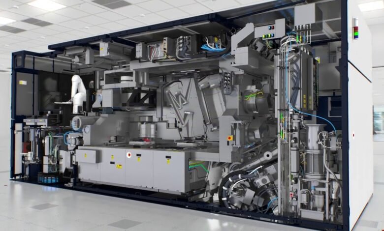
Photolithography and Mask Alignment
As semiconductor devices become more complex and miniaturized, photolithography and mask alignment become increasingly crucial. Advanced photolithography equipment uses shorter wavelengths of light, such as extreme ultraviolet (EUV) light, to achieve nanoscale precision. Mask alignment ensures that multiple semiconductor layers are perfectly aligned, ensuring that the integrated circuits work seamlessly.
Testing and Quality Control
Rigorous testing and quality control measures are enforced throughout the semiconductor manufacturing process. Like electrical testing, surveying electron microscopy( SEM), and X-ray analysis, colorful ways are used to check the wafers for blight and ensure that the bias meets the specifications. Any imperfect factors are repaired or discarded to maintain the quality of the final product.
Packaging and Final Assembly
Once the individual semiconductor devices are manufactured on the wafer, they are cut into individual chips and packaged. The packaging provides protection, electrical connections, and heat dissipation for the semiconductor chip. Packaging varies depending on the application, with options like plastic, ceramic, and ball grid array (BGA) packages.

Conclusion
The semiconductor manufacturing process is a marvel of modern engineering, transforming sand into the silicon chips that power our digital world. Each step is essential in creating the powerful and efficient electronic devices we rely on daily, from the extraction of Silicon to the intricate functions of fabrication, deposition, and doping. As technology advances, so will the semiconductor process, enabling the development of faster, smaller, and more energy-efficient appliances that drive innovation across industries.
FAQs of Semiconductor Manufacturing Process: From Sand to Silicon
What are the crucial raw accouterments used in semiconductor manufacturing?
Silicon is the primary raw material, often sourced from sand. Other materials like dopants, insulators, and conductive materials are also used.
What are the main steps in semiconductor manufacturing?
The main steps include wafer fabrication, deposition, etching, doping, thermal processing, photolithography, mask alignment, testing, quality control, packaging, and final assembly.
How are the tiny electronic components on a semiconductor wafer created?
Photolithography is used to etch intricate patterns onto the silicon wafer, defining the electronic components. A mask and light exposure help create these patterns.
What is doping in semiconductor manufacturing?
Doping is the process of introducing specific impurities (dopants) into the silicon to control its electrical properties. This is essential for creating different types of semiconductor devices.
Semiconductor Manufacturing Process: From Sand to SiliconHow Do You Like Our Post
0


